ENGINEERING JOURNAL
Jingyan Ling
06/27/2019 (Thur)
- Compile
OldRoCorepo- Record of modification:
- ++line 8 of
vstart.sh - -->
pip install -r requirements.txt --user
- ++line 8 of
- Record of modification:
- Export
paperbotdxf file :graph-silhouette.dxftoOnShape- Record of Tips:
- Onshape does not read dxf file as its own saved unit. Manual settings needed when import.

- Record of Tips:
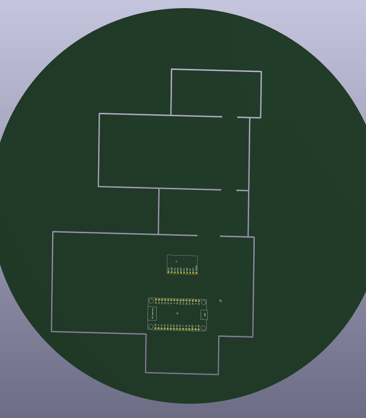
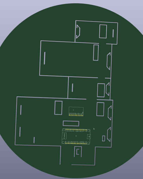
- Draw circuit diagram as CAD on
Onshape- Multiple connection approaches:
-
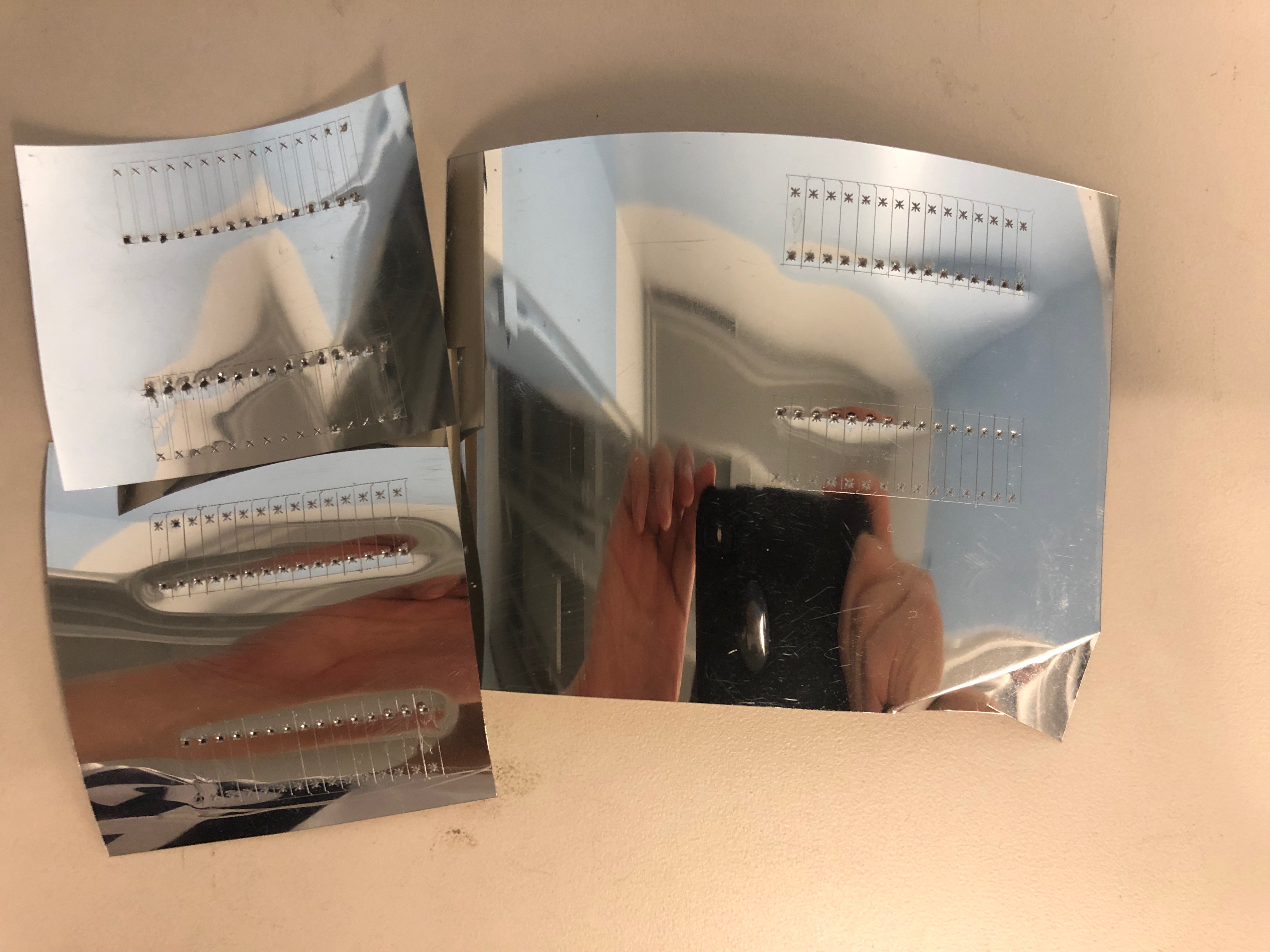
Crossshape of0.039 in -
Crossshape of0.049 in -
Octangularshape of0.049 in
-
- Note and issue:
-
Octangularshape is the best connection approach so far, but none of approach has stable conductivity. More research is needed. - Scratches can be made easily when attaching microcontroller to the sheet. Potential disconnection may occur due to such scratches on metal layer.
- Multiple connection approaches:
- Export 2D CAD drawing with PCB to SVG for silhouette cameo
- Record of Tips:
-
OnShapeunit need to be consisted with unit setting inInkscape(default: mm)
-
- Plugin
Inkscape-silhouettecannot take multiple types of trace for cutting.- Different trace (especially cut and etching) need to be sent separately. Use
coordinate toolofInkscapeto ensure separated cuts have same origin.
- Different trace (especially cut and etching) need to be sent separately. Use
- TODO:
- Cut and etching from same
Inkscapefile
- Cut and etching from same
- Record of Tips:
06/28/2019 (Fri)
Connection and fabrication approach confirmed !
-
Confirm that copper tape has better conductivity than aluminum sheet when attaching microcontroller pins through
H-shapecut- Copper tape is harder to be scratched, which provides less risk of disconnection during assembly.
-
Etching on copper type isolates connections
-
Research on PCB editor
- EAGLE
- EAGLE cannot import
.pcbfile -
svgcan be exported but not imported - Custom library needed if doing schematic design
- EAGLE cannot import
- KiCad
- Can import
.pcbfile -
svgcan be exported but not imported
- Can import
- LayoutEditor
- support multiply file type
-
svgcan be exported with different color makers as multiple layers - include open-sourced auto-router
freerouting
- EAGLE
-
Auto-routing package:
- TopoR
- Python-PCB
- FreeRouting
-
Approaches:
-
A. convert SVG/DXF file to schematic/board design of PCB. Use KiCAD or EAGLE to do auto routing. -
B. develop algorithm on auto routing for single layer svg/dxf file. (path finding problem)
-
Approach A
-
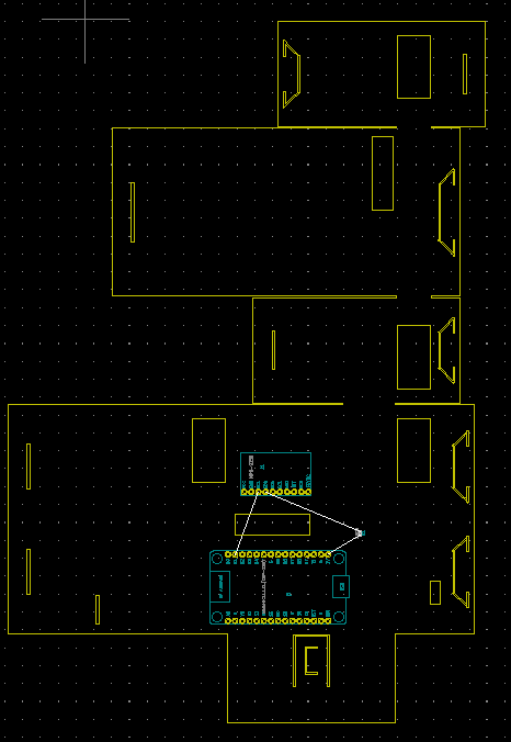
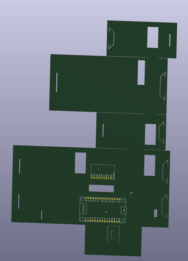
Use regular shape board for PCB in EAGLE/KiCAD
-
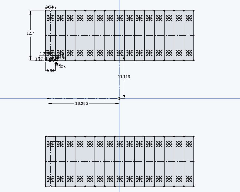
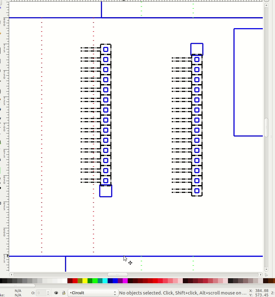
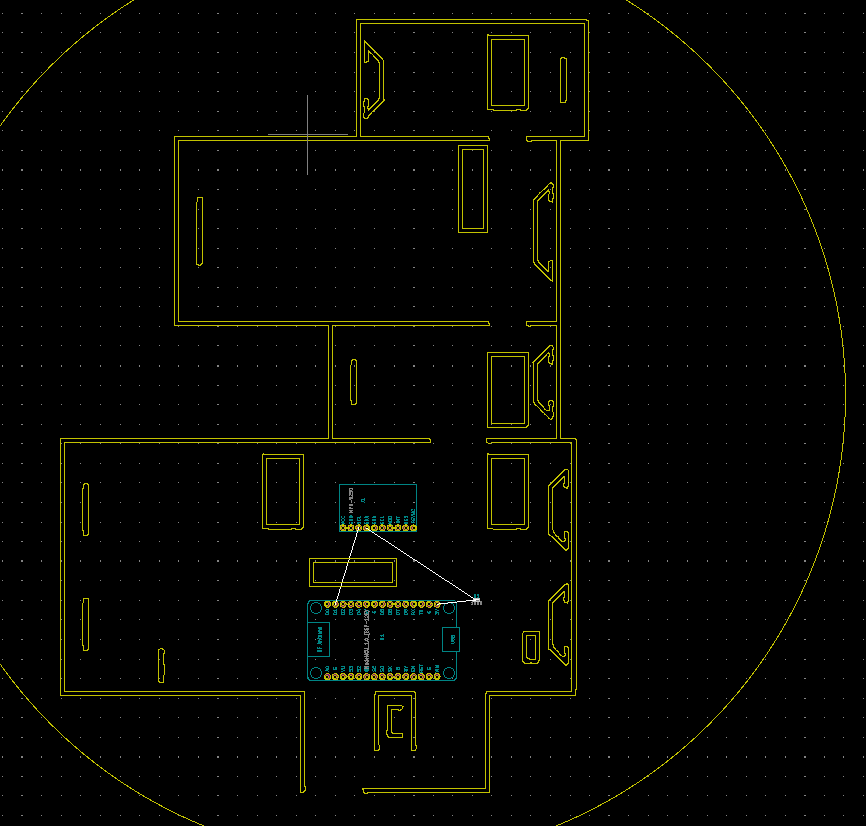
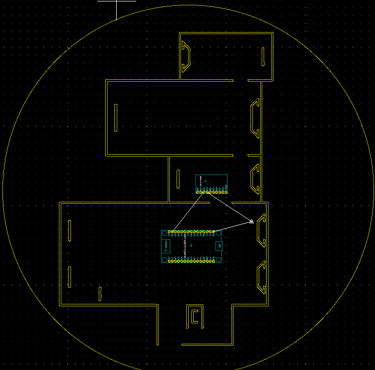
image processing: divide the shape of
paperbotto multiple rectangles (ezdxf) -
Pull required connections and place additional header pins around edges of each rectangle
-
-
Make each connection pin to be two parallel connections so auto-router does parallel trace for each wiring.
- Etching a pair of parallel trace provides isolation, and leave the space between traces to be conductible.
-
Build Library for schematic design
- Schematic design helps with router to know desired connection
- Additional header pins at each side of kink mark
06/29 & 06/30/2019 (Sat & Sun)
Approach B
-
Potential needed functions of packages
- A package draws on DXF file through script
- A script that pulls out pins' coordinate on paper chassis
- Or a image process package (OpenCV) that reads pins' coordinate on paper chassis
- A package solves multi-node path finding problem*
Record of Research
- Python Pathfinding package:
- Python DXF editor:
- ezdxf
-
dxfgrabber
-
Note: able to grab simple geometry from file
-
- sdxf
- Going through tutorials of
ezdxf- All lines on paper space
layer0
- All lines on paper space
07/01/2019 (Mon)
- Continue the dxf processing with
'graph-silhouette.dxf'
Record of tips:
-
Put circuit design on a new layer of dxf drawing
-
Use block feature to draw similar pattern
-
Blocks are
symbolin Inkscape. Convertsymboltopath- Edit > Clone > Unlink Clone (Shift+Alt+D), and you have a group, ungroup (Object > Ungroup, or Shift+Ctrl+G) and edit
-
Convert
texttopath- Path combine (Ctrl+K)
-
msp.delete_enetity('__') to remove existing entity
-
Test fabrication with different drawing settings
- Layers can be cut separately by toggling visibility
- Set cuts with same
intensityandfeedrateon same layer - Entities' layer can be changed through
Entity.dxf.layer
07/02/2019 (Tue)
-
Continue the dxf processing
-
Following tasks can be completed by running the code:
- Able to detect pin center coordinate
- Able to draw arbitrary shape around the pin center
-
-
Issue & TODO
-
Convert dxf image to matrix
-
Explore
pathfindingpackage -
pathfindingpackage solve path finding problem by shortest path algorithm, one point to another -
To solve multiple nodes problem, use concept from reinforcement learning
- Build Q function that represents total reward of choosing certain path to be solved first
- Update Q function in a loop with certain amount of episodes
- Choose the order of solving paths randomly, and add possibility of choosing it from Q function
- Exploration-exploitation method
-
-
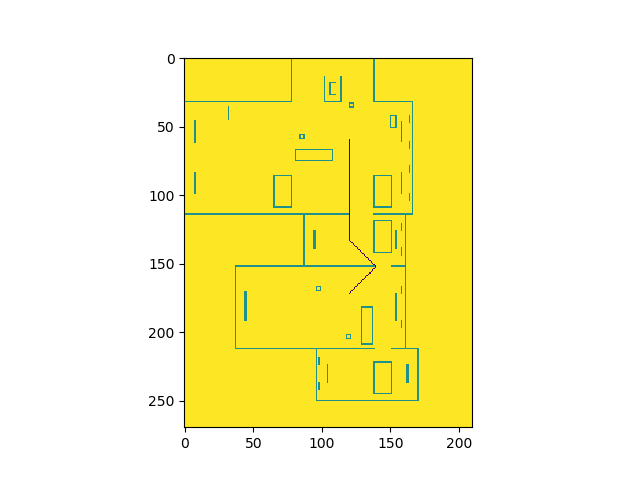
To solve the problem "convert dxf to matrix" for pathfinding:
- Have tried:
- Export to
pngand read file byOpenCV- Resolution problem: single point does not represented as a pixel in
png
- Resolution problem: single point does not represented as a pixel in
- TODO:
- create an empty matrix and fill in numbers with the information of each lines' start and end point
- Export to
- Have tried:
07/03/2019 (Wed)
-
dxf processing completed
-
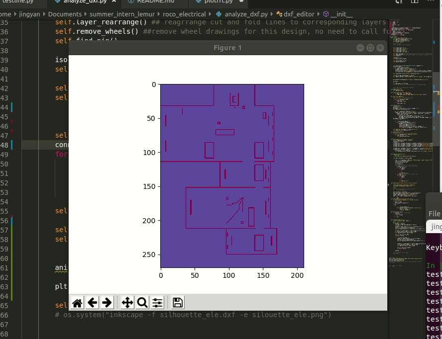
Convert dxf to matrix with resolution (270X210) (mm)
- Potential issue:
- the
pathfindingpackage is based on pixel - When round up the line's start and end point, the accuracy of pin position is low
- the
- Potential issue:
-
Apply single point to point path finding
- Able to draw the path on matrix
- Able to draw the path on original dxf file
-
-
TODO:
- Write out algorithm for multi-node path finding
- break single circuit trace to parallel traces
- solve the accuracy problem
07/05/2019 (Fri)
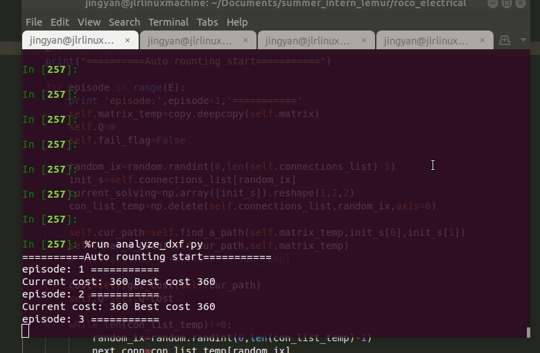
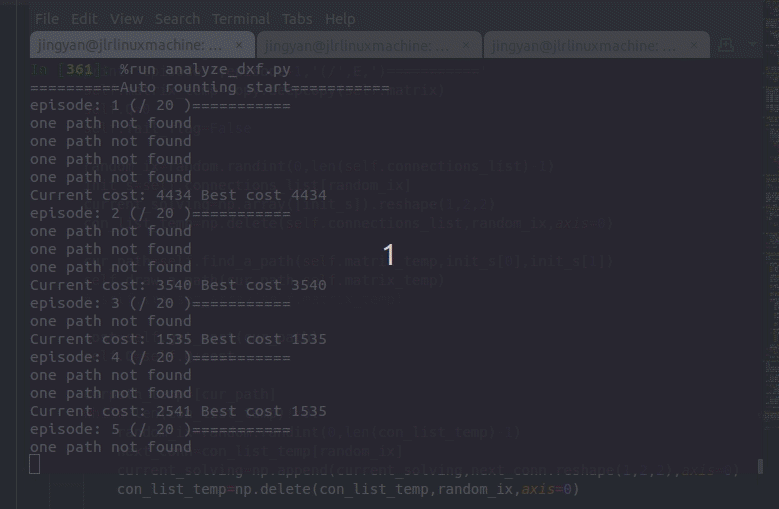
- Write out algorithm for multi-node path finding
- pseudo code:
 for (episode in E):
    set initial state s (choose first pair of nodes to connect randomly)
    find a path
    update map
    while not every connection is built:
      choose next connection
      find a path
      update map
      retrieve cost (length of path)
    update Q (as sum of all cost)
-
Q here represents total cost of certain choice of path finding order.
- Cost defined by length of path
- If path cannot be found, cost 1000
-
Input: NX2X2 array specifies desired pin connections
-
Research on KiCAD import needs and python API
07/08/2019 (Mon)
- Debug multi-node path finding:
- some obstacles are ignored
- too close to each other
- Able to show the learning process:
- Trying different combination of solving order
- Try to give the best order of solving multiple path
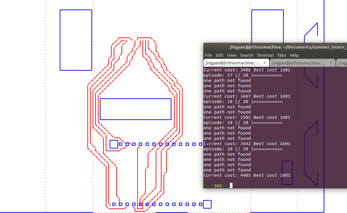
Auto-routing learning process:
-
-
Comparison between episodes and choose best combo of paths
-
Issues and TODO
- Path export from optimization is messed up
- Obstacles setting are incorrect
07/09/2019
-
Finish up path-finding approach (Approach B)
-
Only draw the best path on
dxfwhen solution is found for every route. -
-
Throw warning once a route cannot be found
-
-
Research on Approach A
-
KiCAD 5 does not have built-in auto-router
- Have to use
FreeRouting
- Have to use
-
FreeRoutingdoes not have python API -
Parent package of
FreeRouting,LayoutEditorhas multiple editions- Part of
LayoutEditoris open- source - A large amount of of its website are broken, source and interface are unavailable
- Part of
-
-
Other auto-routers are not open-source
Approach A
-
- Use
LayoutEditorpython API to useFreeRouting
- Use
-
- Use
KiCAD 5python API to sueFreeRouting
- Use
-
- Use
KiCAD 4python API to use builtin auto-routing
- Use
1
-
FreeRoutinginput format:dsn,lef,def -
FreeRoutingoutput format:ses,def -
FreeRoutingcan take arbitrary board outlines shape -
Edit
librarymanually and test routing -
-
TODO:
- If can run KiCAD 4 from python
- Check
FreeRoutingAPI, see if a acceptable file can be generated from things on hand
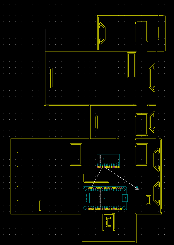
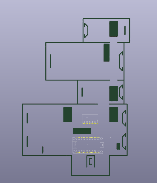
07/10/2019
Approach A
-
Import to PCBnew issue:
- Dimension of board outlines are incorrect
- Pins does not fit in original drawings
- (solved. Microcontroller footprint was incorrect)
-
pipeline confirmed:
-
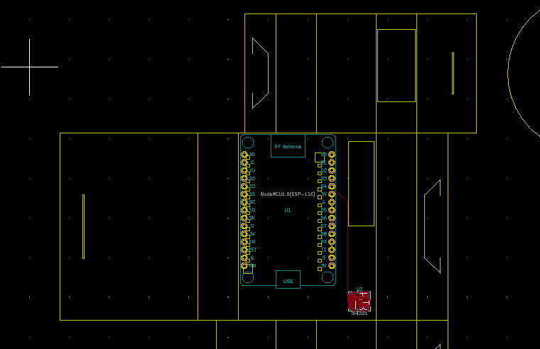
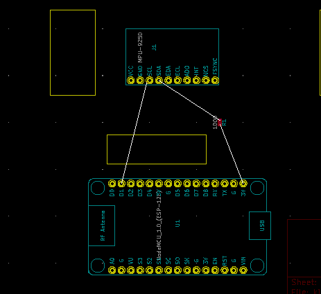
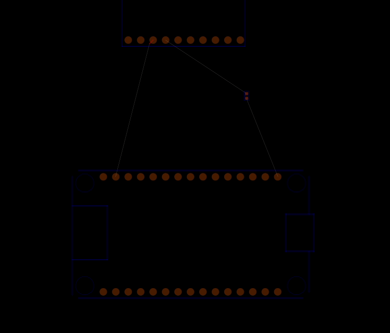
- Build symbol and footprint library for all required electrical element
-
- Sketch schematic design
-
.schfile
-
- Place elements in required position
-
.dsnfile
-
- Import
dsnfile intoFreeRoutingand do auto-routing
-
.sesfile
- Import
-
- Import
sesfile back toKiCADand export asdxffile
-
.dxffile
- Import
-
-
Manually tested pipeline till step 4
-
Step 3
-
-
Step 4
-
-
ISSUE:
- Board outlines are not exported correctly to
FreeRouting - Error:
unable to find segment with an endpoint
- Board outlines are not exported correctly to
-
Record of Tips:
- To run
FreeRoutingfrom command line:java -jar freeRouting.jar [proj.dsn]
- To run
-
-
TODO:
- Finish with testing the pipeline manually
- Achieve steps directly from script (Python API)
07/11/2019
-
Solved Error
unable to find segment with an endpoint-
DSNfile can only be exported for continuous closure outlines -
-
Drawings like this drawing for paper cut is not acceptable for
dsnfile. -
Change it either to close shape or remove it when import to KiCAD
-
-
Solving Issue:
FreeRoutingis not reading edge cut layer fromdsn- Work well on a sample
dsnfile - Issue with KiCAD output
- Sample KiCAD project can output outlines properly.
- Work well on a sample
-
Issue found:
- KiCAD cannot take single line cut. Closed shape needed.
07/15/2019
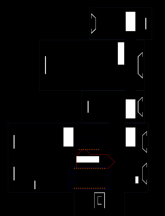
-
3 potential ways to solve the issue on KiCAD with internal cut
-
Assume the position of each internal cut line is known
-
- Make internal cut a closed shape (original cut with thickness)
- Pro: Easy to import routed circuit back to dxf cutter file
- Con: Hard to make the cut itself a closed shape.
-
- Make internal cut outlines a block on certain layer and treat it as obstacle in auto-router
- Pro: Easy to generate a block as obstacle in drawing
- Con: Hard to import routed circuit back to dxf cutter file
-
- Put internal cut on different layer in KiCAD that can be read as obstacle in auto-router
- Best solution for now if the auto-router will be able to read single cut line, but cannot be edge.cut layer for sure, otherwise board outlines cannot be found by KiCAD.
-
-
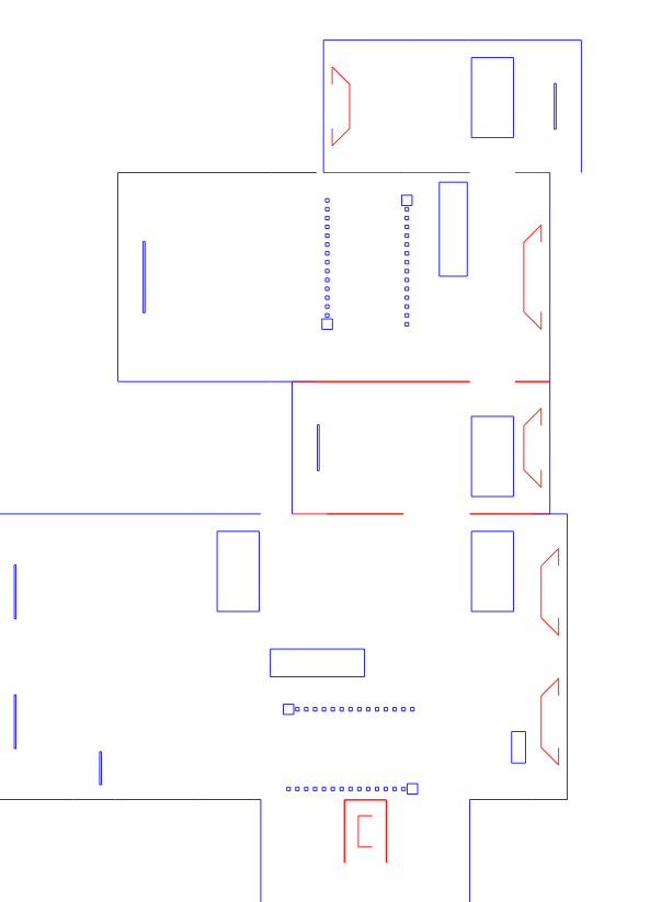
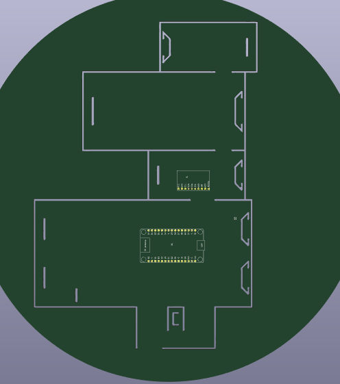
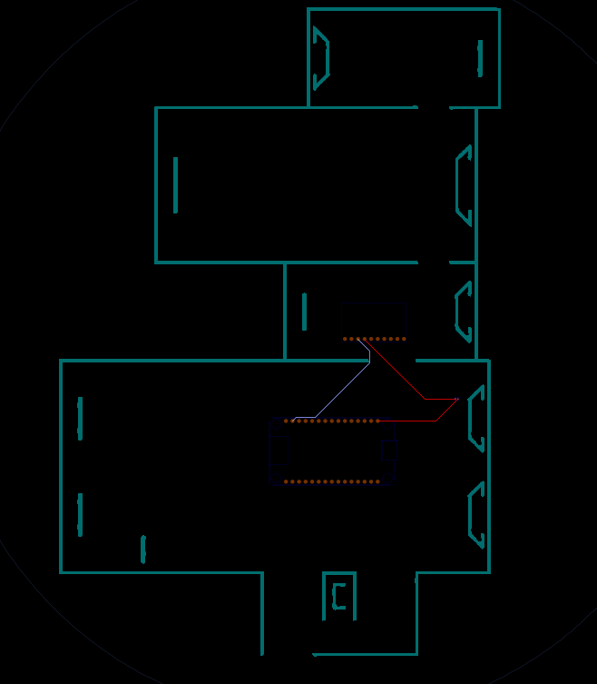
Cut lines causing issues are marked in red.
-
-
Inkscape:- Object stroke to path can make everything looks like a bounding box
-
Attempts:
-
- Stroke every line, auto-router shows nothing, no error
-
-
-
- Stroke every line, but has a larger boundary. auto-router shows nothing, error: cannot start a route inside of keepout area or boundary outlines
-
-
-
- Stroke every line but make the boundary outlines not closed, and draw a larger outline. Auto-router shows nothing, no error
-
-
-
- Stroke only outline but make the boundary outlines not closed, and draw a larger outline. Auto-router shows properly. (no way to do it from script)
-
-
-
07/16/2019
-
Fill and Stroke (Shift + Ctrl + F)
-
Stroke to Path
-
Union
-
Break Apart
-
Remove each outer layer (manually)
-
Export
-
-
-
-
Consider success when export for auto-routing manually. Huge challenge expected when doing it from script.
-
Work on script doing schematic design
- Assume symbol and footprint downloaded
- Package Using: skidl
- Record of Tips:
- Add custom library path that contains all symbols of electrical devices needed (
NodeMCU) - Use attribute
footprintto add footprint for such symbol - footprint syntax: 'footprint= libname.pretty: foot_print_name
- footprint directory should be under the same directory where
.libfile is.
- Add custom library path that contains all symbols of electrical devices needed (