## ENGINEERING JOURNAL
### Jingyan Ling
### 08/06/2019
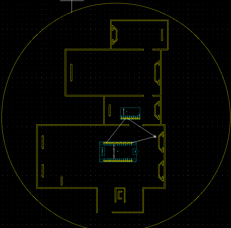
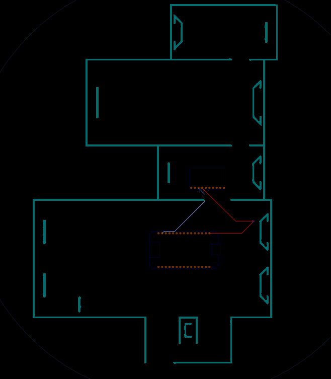
- Successfully parse the wiring information from `ses` file to array
- A little "hacky" way, not using any parsing package but going through string and looking for path section
- For `ses` file only
- Create new scripts and Re-arrange all packages
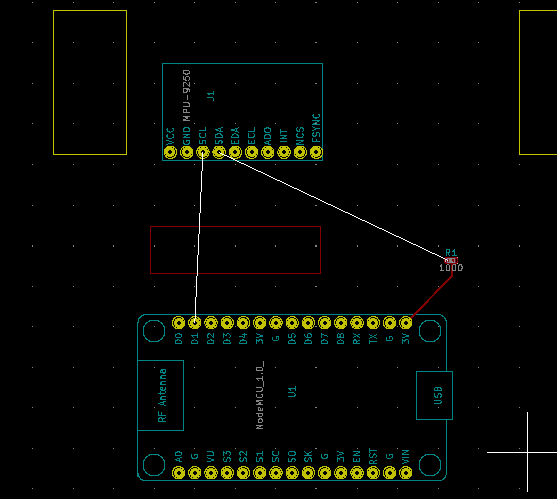
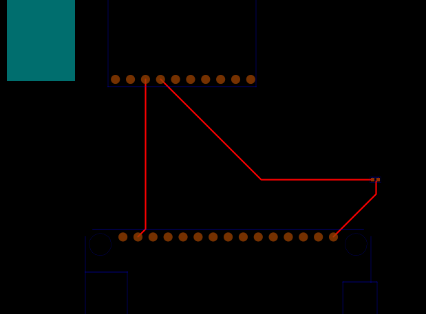
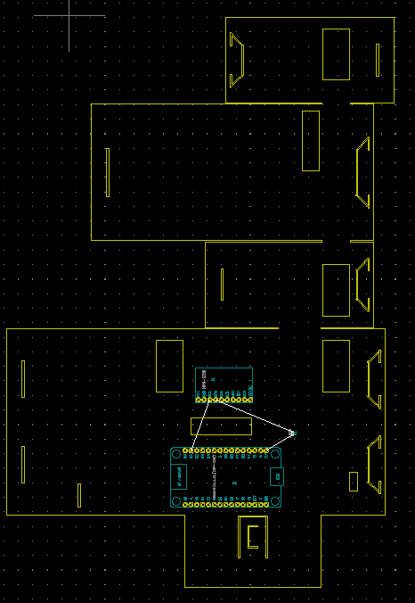
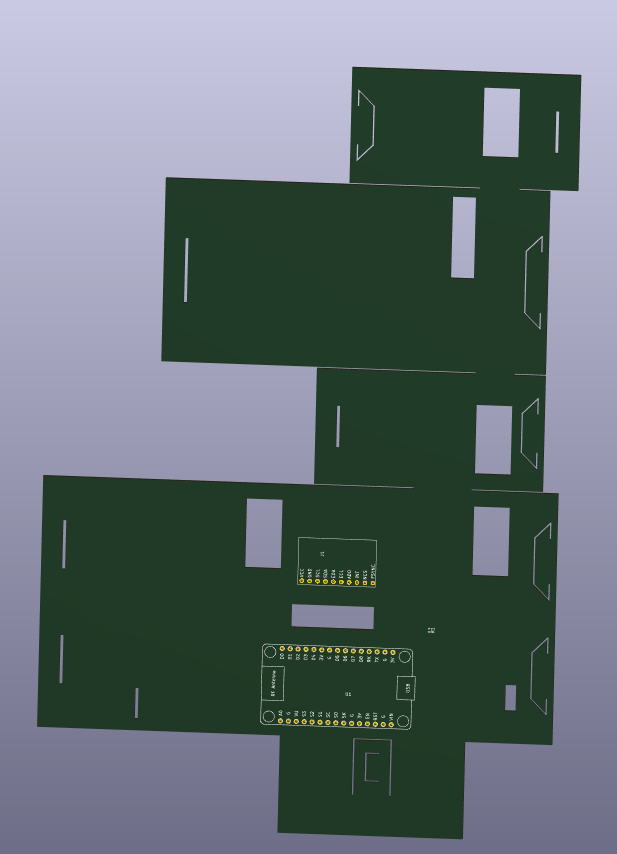
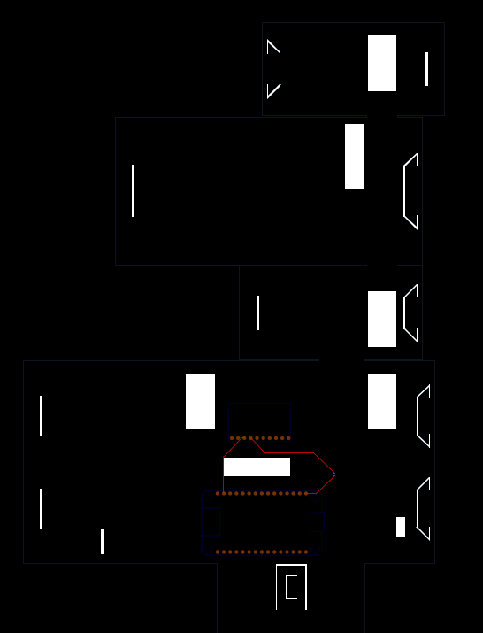
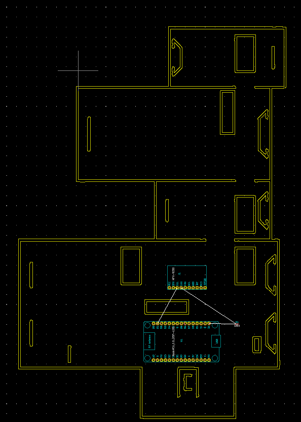
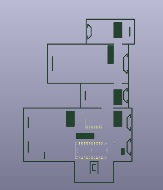
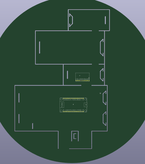
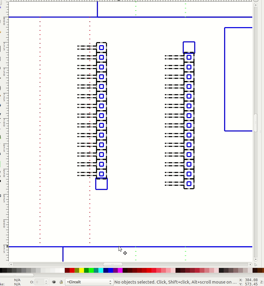
- User will be able to execute [fab_drawing.py](paperbot_ee_autoroute/fab_drawing.py) directly to get drawing for paperbot including electrical wiring design and ready to send to fabrication
- If user wants to change electrical connection, one can edit [paperbot_dsn.py](paperbot_ee_autoroute/paperbot_dsn.py)
- `dsnwriter` and `sesreader` source code are located [here](dsn_python/)
- New script:
- [paperbot_draw.py](paperbot_ee_autoroute/paperbot_draw.py) has two classes:
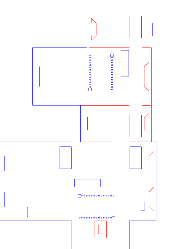
- `pre-process`
- process the mechanical design drawing to correct format that can be taken by `dsnwriter` and `autorouter`
- `post-process`
- process the drawing file and draw wires based on `ses` file generated from `autorouter`
- Milestone:
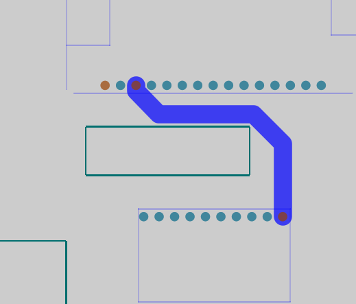
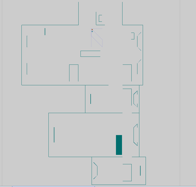
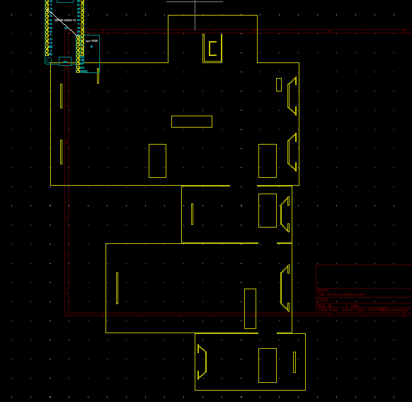
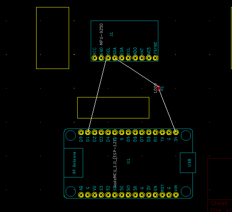
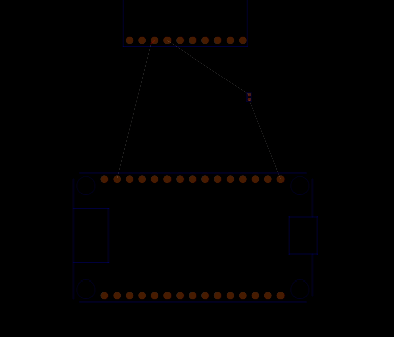
- Now user can generate `dsn` file from script and confirm auto-routing.
- A parser can pull information for wiring
- Able to draw such wiring back on `dxf` drawings
- 
- TODO:
- Merge pre drawing processing script with Daniel
- Details:
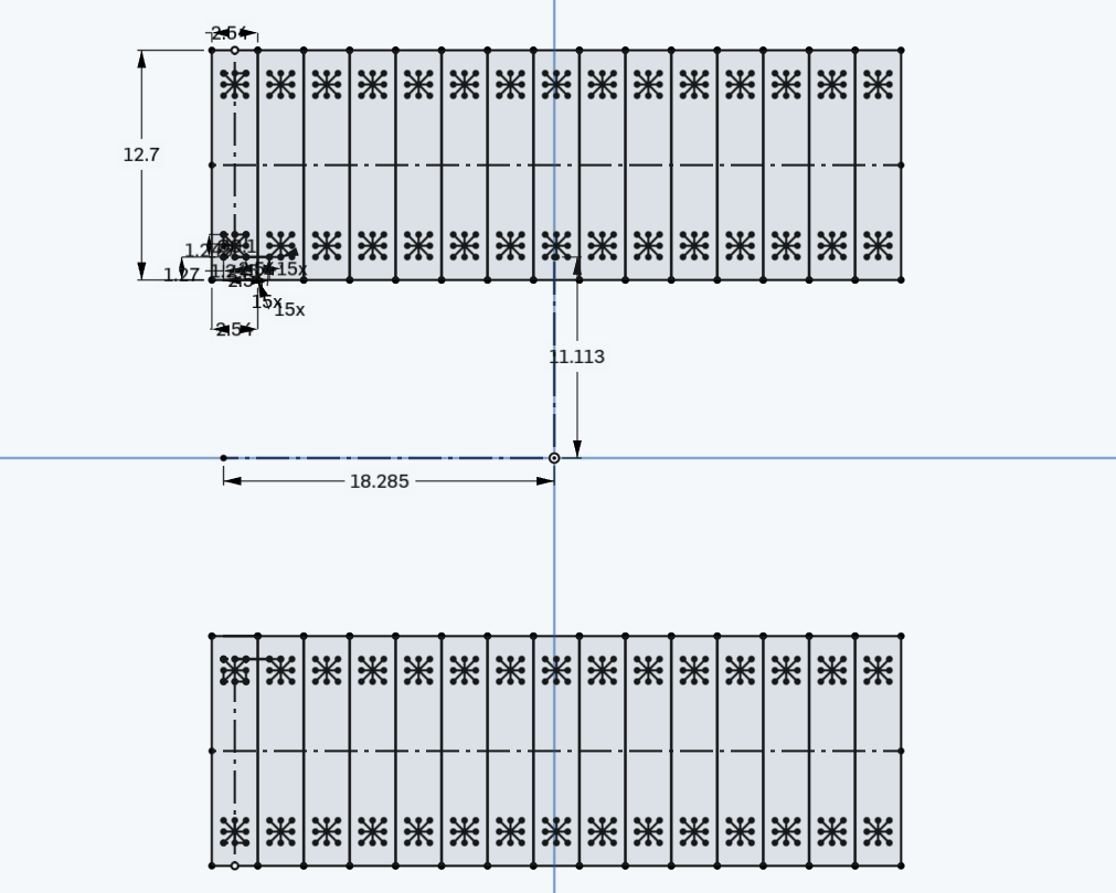
- add 'cross-cut' block in `ezdxf` for pin insertion cut
- add 'parallel-trace' block in` ezdxf` for circuit trace on copper tape
### 08/05/2019
- Working on parsing routed (wiring section) text information.
- Ref: [pyparsing](https://scipy-cookbook.readthedocs.io/items/Reading_Custom_Text_Files_with_Pyparsing.html)
- Parsing generated `dsn` file back to `DSN` class
- Fail
- Parsing generated `kicad_pcb` file back to `pykicad` package - `pcb` class
- Success
- Working on:
- debug dsn library so it can read file.
- `pykicad` uses `pyparsing` internally
- Rebuild `ses` file schema. Not working well
### 08/01/2019
- Scripting Auto-router from python
- Run `.jar` package through python
- Can open GUI with imported file
- Cannot run auto-routing function from script
- Manually click on auto-routing and save is needed (manual approval)
### 07/31/2019
- Use `dsnwriter` in RoCo
~~~
Mechanical drawings (dxf/svg)------------|
|
Module Footprints -----------------------|
|----> board design (dsn)
Electrical schematic design (netlist)----|
|
Board design details(rules,parameters)---|
----> board design (dsn)----> Auto-router (FreeRouting)----> routed board design (dsn)
----> wiring section ----> drawings with mechanical and electrical design (dxf/svg)
~~~
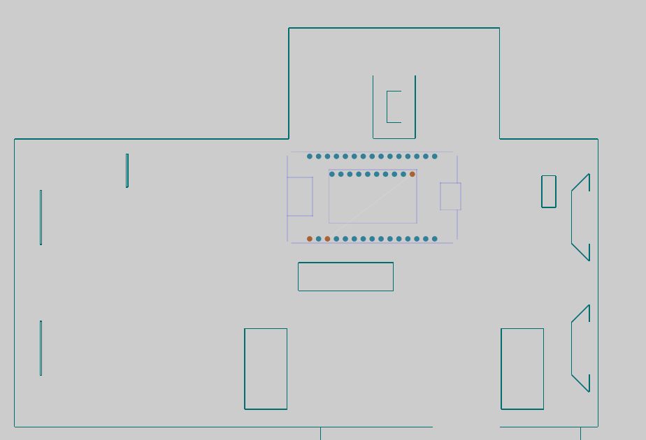
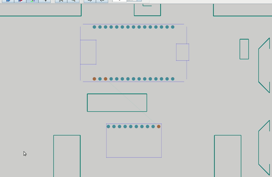
- The package now can auto-detect padstack information with multiple files
### 07/30/2019
- Record of Tips:
- Use `@classmethod` in class to parse information pull out from files (netlist,drawings,footprint) to original class
- Package Dependencies:
- [pykicad](https://github.com/dvc94ch/pykicad)
- numpy
- Class Footprint now can call function `from_file(path,ref)` to load footprint from a `.kicad_mod` file
- Class Padstack now can call function 'auto_detact(path)` to guess information of pads and save as padstack class
- Via information need to be defined by users. (default=None)
- Placement class can be defined after footprint is loaded and able to define the position of each component by calling `ref` of module.
- 
- 
- Netclass is easy to write from script.
- Test auto-routing on generated `dsn`
- 
- Test on wire width change
- 
- TODO: Easier API to generate netlist.
### 07/29/2019
- Was working on 'dsn_python' Python Library.
- Latest package can be found at [personal github](https://github.com/monkalynn813/dsn_python)
- Class tree:
~~~
|--dsnwritter.py (top and second level structure)
|--dsn_module.py
|--module class
|--load module functions
|--dsn_rule.py
|--dsn_geo.py
|--boundary class
|--keepout class
|--load drawing functions
|--dsn_net.py
|--net class
|--netclass class
|--load netlist functions
~~~
- Text tree structure is done.
- Documentation and notes for code needed
- Functions are needed to help user use library.
- Function that load `dxf` file
- Function that load `footprint` file
- Function that load `netlist` file
- For board outline/footprint/netlist not loaded from file but define through this library manually, it works very well for now.
- Pull out those information from low-level file and convert it to proper text for `dsn` file
- Record of Tips:
- `Freerouting` cannot take more than one boundary. (error: exact 1 bounding expected)
- Able to use functions to load `dxf` drawings
- "internal cut issue" solved
- Treat every line individually as polygon and labeled as keepout in `dsn` library
- 
- 
### 07/24/2019
- Pipeline change: (skipping `KiCAD`)
- Use (`dxf`+ `pretty` (footprint library) + `net` information ) to generate `dsn` file
- Send `dsn` file to auto-router, save as new `dsn` file
- Read `dsn` file `wiring` information and draw it back on `dxf`
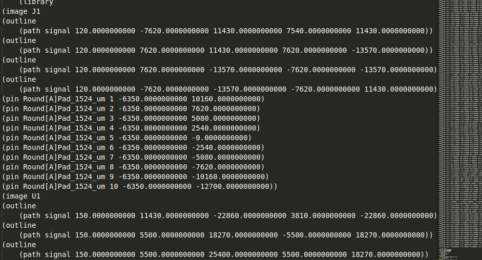
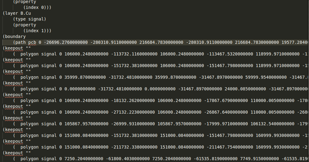
- Analysis on `dsn` file format:
~~~
|--pcb
| |--parser
| |--resolution
| |--unit
| |--structure
| | |--layer 1
| | |-- ...
| | |--boundary
| | |--keepout 1
| | |-- ...
| | |--via
| | |--rule
| |--placement
| | |--component 1
| | |-- ...
| |--library
| | |--image [ref**] 1
| | | |--outline
| | | |--pin
| | |-- ...
| | |--padstack
| | |--...
| |--network
| | |--net [name] 1
| | | |--pins
| | |-- ...
| |--wiring
| | |--wire
~~~
- TODO: functions that load modules and footprints
### 07/23/2019
- Solving issue: export `.kicad_brd` file to `dsn` file for auto-router
- No known Python API so far.
- [schematic-file-converter](https://github.com/ljmljz/schematic-file-converter)
- Take `.sch` file from `KiCAD` instead of `.kicad_brd` file
- Official bug report has been requested. Not targeted in current `KiCAD` scripting version
- [bug report](https://bugs.launchpad.net/kicad/+bug/1824668)
- Potential Solutions:
- 1. Explore existing supported export API, and see if modification can be made based on existing API structure
- 2. Learn `dsn` file specification and python library to generate `dsn` file based on design information
### 07/22/2019
- Research on multiple KiCAD Python packages
- [package 3rd party list](https://github.com/xesscorp/kicad-3rd-party-tools/blob/master/README.md#footprint-library-tools)
- None can import `dxf` into `pcbnew`
- To import `dxf` into `pcbnew` automatically:
- Create a python API by myself based on the `c++` code
- Draw lines directly in `pcbnew` by using line information in `dxf`
- Create a python script serving as Python API by drawing everything on `pcbnew`
- Dependencies:
- ezdxf
- pykicad
- Successfully import `dxf` as outlines from script
- 
### 07/18/2019
- Research on pcbnew API
- Using package [pykicad](https://github.com/dvc94ch/pykicad)
- Record of Tips:
- Do not add segments, which will route connections
- Different reference name need to be set for `dsn` export
- Able to add footprint and net list into pcbnew.
- TODO:
- Import dxf as outlines from script
- Export board as `dsn`
### 07/17/2019
- Notice that even the drawings cannot be imported onto 'wiring' layer, but can be changed manually to 'wiring' layer after importing onto 'edge.cut' layer
- `Freerouting` does not recognize wires that does not connect to any pins as obstacles.
- 
- 
- Work on script doing board design
- Create New Board
- Import DXF
- Load Netlist `.net` file
- Place modules
- Export to `.dsn` file
### 07/16/2019
- Fill and Stroke (Shift + Ctrl + F)
- Stroke to Path
- Union
- Break Apart
- Remove each outer layer (manually)
- Export
- 
- 
- 
- Consider success when export for auto-routing manually. Huge challenge expected when doing it from script.
- Work on script doing schematic design
- *Assume symbol and footprint downloaded*
- Package Using: [skidl](https://xesscorp.github.io/skidl/docs/_site/)
- Record of Tips:
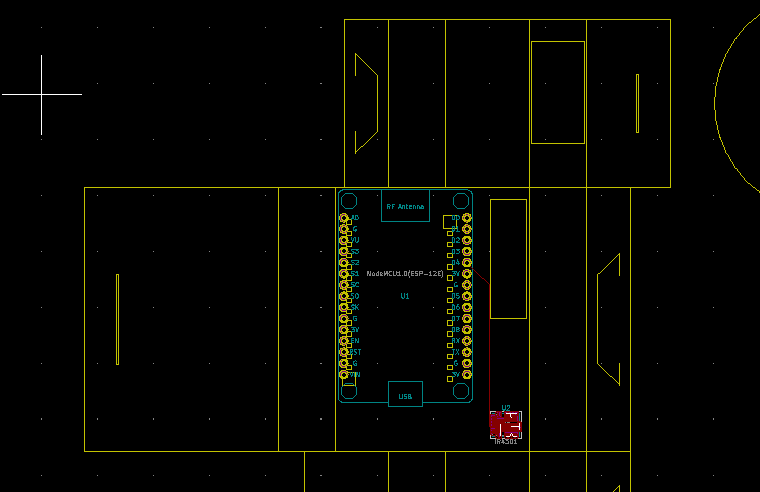
- Add custom library path that contains all symbols of electrical devices needed (`NodeMCU`)
- Use attribute `footprint` to add footprint for such symbol
- footprint syntax: 'footprint= libname.pretty: foot_print_name
- footprint directory should be under the same directory where `.lib` file is.
### 07/15/2019
- 3 potential ways to solve the issue on KiCAD with internal cut
- *Assume the position of each internal cut line is known*
- 1. Make internal cut a closed shape (original cut with thickness)
- Pro: Easy to import routed circuit back to dxf cutter file
- Con: Hard to make the cut itself a closed shape.
- 2. Make internal cut outlines a block on certain layer and treat it as obstacle in auto-router
- Pro: Easy to generate a block as obstacle in drawing
- Con: Hard to import routed circuit back to dxf cutter file
- 3. Put internal cut on different layer in KiCAD that can be read as obstacle in auto-router
- Best solution for now if the auto-router will be able to read single cut line, but cannot be edge.cut layer for sure, otherwise board outlines cannot be found by KiCAD.
- Cut lines causing issues are marked in red.
- 
- `Inkscape` :
- Object stroke to path can make everything looks like a bounding box
- Attempts:
- 1. Stroke every line, auto-router shows nothing, no error
- 
- 
- 2. Stroke every line, but has a larger boundary. auto-router shows nothing, error: cannot start a route inside of keepout area or boundary outlines
- 
- 
- 3. Stroke every line but make the boundary outlines not closed, and draw a larger outline. Auto-router shows nothing, no error
- 
- 
- 4. Stroke only outline but make the boundary outlines not closed, and draw a larger outline. Auto-router shows properly. (no way to do it from script)
- 
- 
- 
### 07/11/2019
- Solved Error `unable to find segment with an endpoint`
- `DSN` file can only be exported for continuous closure outlines
- 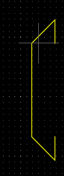
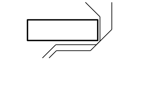
- Drawings like this drawing for paper cut is not acceptable for `dsn` file.
- Change it either to close shape or remove it when import to KiCAD
- Solving Issue: `FreeRouting` is not reading edge cut layer from `dsn`
- Work well on a sample `dsn` file
- Issue with KiCAD output
- Sample KiCAD project can output outlines properly.
- Issue found:
- KiCAD cannot take single line cut. Closed shape needed.
### 07/10/2019
##### Approach A
- Import to PCBnew issue:
- Dimension of board outlines are incorrect
- Pins does not fit in original drawings
- (solved. Microcontroller footprint was incorrect)
- pipeline confirmed:
- 1. Build symbol and footprint library for all required electrical element
- 2. Sketch schematic design
- `.sch` file
- 3. Place elements in required position
- `.dsn` file
- 4. Import `dsn` file into `FreeRouting` and do auto-routing
- `.ses` file
- 5. Import `ses` file back to `KiCAD` and export as `dxf` file
- `.dxf` file
- Manually tested pipeline till step 4
- Step 3
- 
- Step 4
- 
- ISSUE:
- Board outlines are not exported correctly to `FreeRouting`
- Error: `unable to find segment with an endpoint`
- Record of Tips:
- To run `FreeRouting` from command line:
~~~
java -jar freeRouting.jar [proj.dsn]
~~~
- TODO:
- Finish with testing the pipeline manually
- Achieve steps directly from script (Python API)
### 07/09/2019
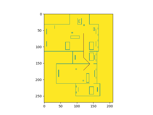
- Finish up path-finding approach (Approach B)
- Only draw the best path on `dxf` when solution is found for every route.
- 
- Throw warning once a route cannot be found
- 
- Research on Approach A
- KiCAD 5 does not have built-in auto-router
- Have to use `FreeRouting`
- `FreeRouting` does not have python API
- Parent package of `FreeRouting`, `LayoutEditor` has multiple editions
- Part of `LayoutEditor` is open- source
- A large amount of of its website are broken, source and interface are unavailable
- Other auto-routers are not open-source
##### Approach A
- 1. Use `LayoutEditor` python API to use `FreeRouting`
- 2. Use `KiCAD 5` python API to sue `FreeRouting`
- 3. Use `KiCAD 4` python API to use builtin auto-routing
###### 1
- `FreeRouting` input format: `dsn`, `lef`, `def`
- `FreeRouting` output format: `ses`, `def`
- `FreeRouting` can take arbitrary board outlines shape
- Edit `library` manually and test routing
- 
- TODO:
- If can run KiCAD 4 from python
- Check `FreeRouting` API, see if a acceptable file can be generated from things on hand
### 07/08/2019 (Mon)
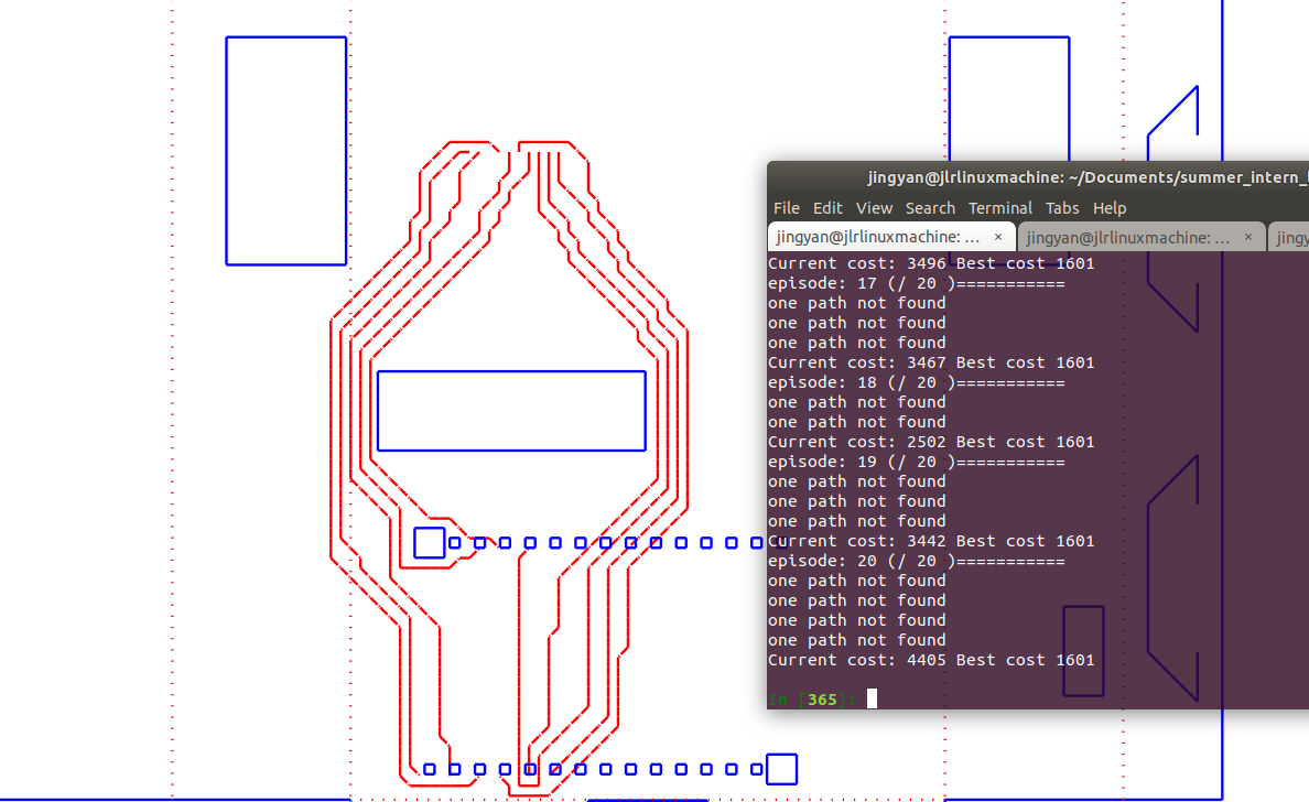
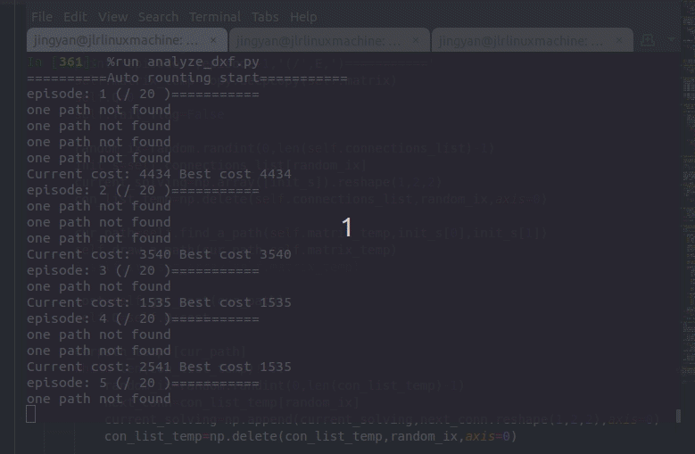
- Debug multi-node path finding:
- some obstacles are ignored
- too close to each other
- Able to show the learning process:
- Trying different combination of solving order
- Try to give the best order of solving multiple path
##### Auto-routing learning process:
- 
- Comparison between episodes and choose best combo of paths
- 
##### Issues and TODO
- Path export from optimization is messed up
- Obstacles setting are incorrect
### 07/05/2019 (Fri)
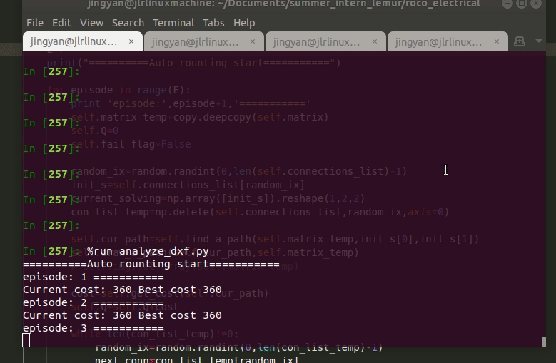
- Write out algorithm for multi-node path finding
- pseudo code:
~~~~
for (episode in E):
set initial state s (choose first pair of nodes to connect randomly)
find a path
update map
while not every connection is built:
choose next connection
find a path
update map
retrieve cost (length of path)
update Q (as sum of all cost)
~~~~
- Q here represents total cost of certain choice of path finding order.
- Cost defined by length of path
- If path cannot be found, cost 1000
- Input: NX2X2 array specifies desired pin connections
- Research on KiCAD import needs and python API
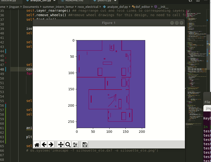
### 07/03/2019 (Wed)
- dxf processing completed
- Convert dxf to matrix with resolution (270X210) (mm)
- Potential issue:
- the `pathfinding` package is based on pixel
- When round up the line's start and end point, the accuracy of pin position is low
- Apply single point to point path finding
- Able to draw the path on matrix
- Able to draw the path on original dxf file
- 
- TODO:
- Write out algorithm for multi-node path finding
- break single circuit trace to parallel traces
- solve the accuracy problem
### 07/02/2019 (Tue)
- Continue the dxf processing
- Following tasks can be completed by running the code:
- Able to detect pin center coordinate
- Able to draw arbitrary shape around the pin center
- 
- - Issue & TODO
- Convert dxf image to matrix
- Explore `pathfinding` package
- `pathfinding` package solve path finding problem by shortest path algorithm, one point to another
- To solve multiple nodes problem, use concept from reinforcement learning
- Build Q function that represents total reward of choosing certain path to be solved first
- Update Q function in a loop with certain amount of episodes
- Choose the order of solving paths randomly, and add possibility of choosing it from Q function
- Exploration-exploitation method
- To solve the problem "convert dxf to matrix" for pathfinding:
- Have tried:
- Export to `png` and read file by `OpenCV`
- Resolution problem: single point does not represented as a pixel in `png`
- TODO:
- create an empty matrix and fill in numbers with the information of each lines' start and end point
### 07/01/2019 (Mon)
- Continue the dxf processing with `'graph-silhouette.dxf'`
##### Record of tips:
- Put circuit design on a new layer of dxf drawing
- [check doc about layers here](https://ezdxf.readthedocs.io/en/latest/tutorials/layers.html)
- Use block feature to draw similar pattern
- [check doc about block here](https://ezdxf.readthedocs.io/en/latest/tutorials/blocks.html)
- Blocks are `symbol` in Inkscape. Convert `symbol` to `path`
- Edit > Clone > Unlink Clone (Shift+Alt+D), and you have a group, ungroup (Object > Ungroup, or Shift+Ctrl+G) and edit
- Convert `text` to `path`
- Path combine (Ctrl+K)
- msp.delete_enetity('__') to remove existing entity
- Test fabrication with different drawing settings
- Layers can be cut separately by toggling visibility
- Set cuts with same `intensity` and `feedrate` on same layer
- Entities' layer can be changed through `Entity.dxf.layer`
### 06/29 & 06/30/2019 (Sat & Sun)
##### Approach `B`
- Potential needed functions of packages
- A package draws on DXF file through script
- A script that pulls out pins' coordinate on paper chassis
- Or a image process package (OpenCV) that reads pins' coordinate on paper chassis
- A package solves multi-node path finding problem*
##### Record of Research
- Python Pathfinding package:
- [pathfinding](https://pypi.org/project/pathfinding/#description)
- Python DXF editor:
- [ezdxf](https://pypi.org/project/ezdxf/)
- [dxfgrabber](https://pypi.org/project/dxfgrabber/)
- `Note`: able to grab simple geometry from file
- [sdxf](http://www.kellbot.com/sdxf-python-library-for-dxf/)
- Going through tutorials of `ezdxf`
- All lines on paper space`layer0`
### 06/28/2019 (Fri)
##### Connection and fabrication approach confirmed !
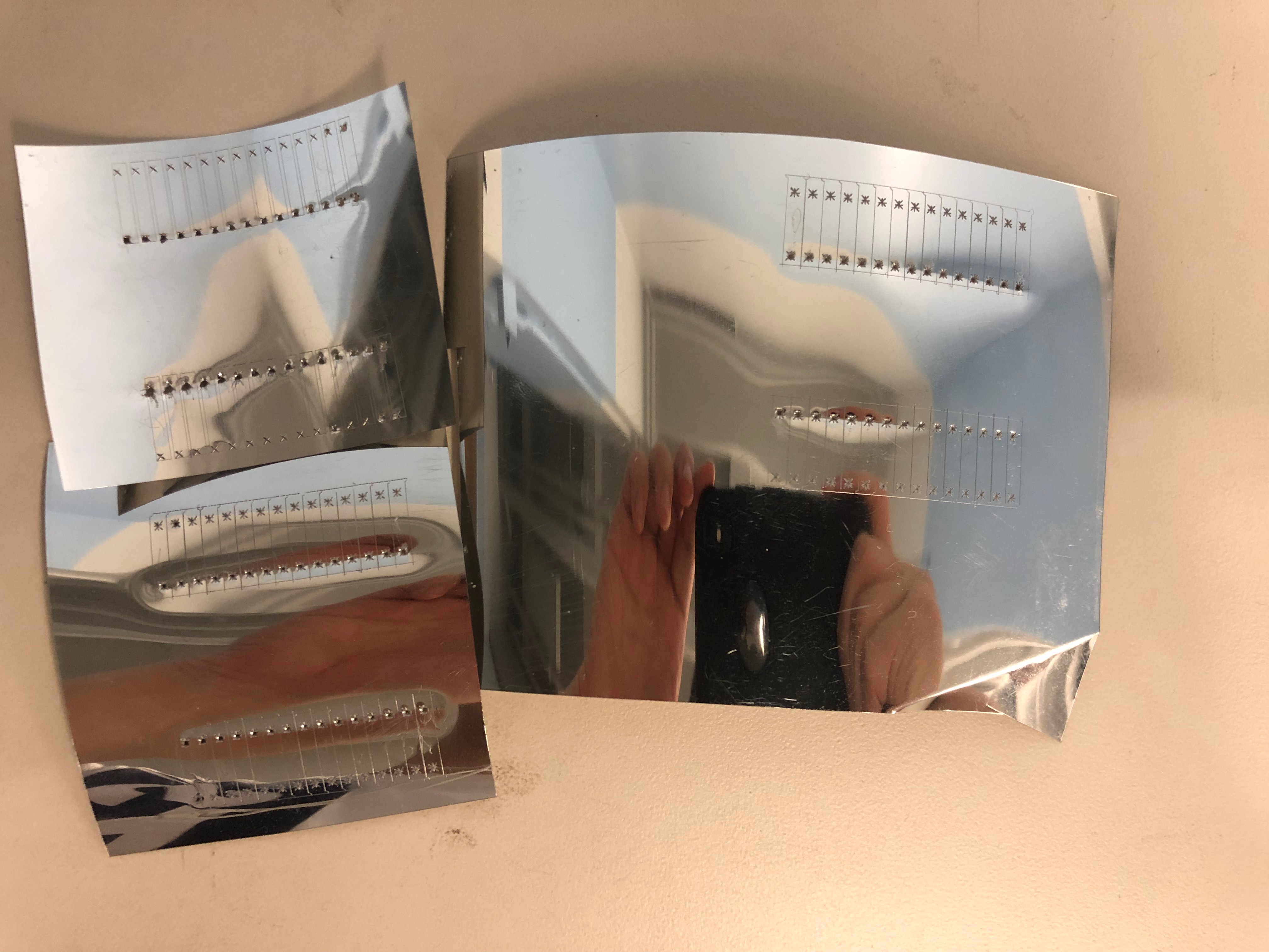
- Confirm that copper tape has better conductivity than aluminum sheet when attaching microcontroller pins through `H-shape` cut
- Copper tape is harder to be scratched, which provides less risk of disconnection during assembly.
- Etching on copper type isolates connections
- Research on PCB editor
- EAGLE
- EAGLE cannot import `.pcb` file
- `svg` can be exported but not imported
- Custom library needed if doing schematic design
- KiCad
- Can import `.pcb` file
- `svg` can be exported but not imported
- LayoutEditor
- support multiply file type
- `svg` can be exported with different color makers as multiple layers
- include open-sourced auto-router `freerouting`
- Auto-routing package:
- TopoR
- Python-PCB
- FreeRouting
- Approaches:
- `A`. convert SVG/DXF file to schematic/board design of PCB. Use KiCAD or EAGLE to do auto routing.
- `B`. develop algorithm on auto routing for single layer svg/dxf file. (path finding problem)
##### Approach `A`
- Use regular shape board for PCB in EAGLE/KiCAD
- image processing: divide the shape of `paperbot` to multiple rectangles (ezdxf)
- Pull required connections and place additional header pins around edges of each rectangle
- Make each connection pin to be two parallel connections so auto-router does parallel trace for each wiring.
- Etching a pair of parallel trace provides isolation, and leave the space between traces to be conductible.
- Build Library for schematic design
- Schematic design helps with router to know desired connection
- Additional header pins at each side of kink mark
### 06/27/2019 (Thur)
- Compile `OldRoCo` [repo](https://git.uclalemur.com/mehtank/oldroco)
- Record of modification:
- ++line 8 of `vstart.sh`
- --> `pip install -r requirements.txt --user`
- Export `paperbot` dxf file : `graph-silhouette.dxf` to `OnShape`
- Record of Tips:
- Onshape does not read dxf file as its own saved unit. Manual settings needed when import.
- 
- Draw circuit diagram as CAD on `Onshape`
- Multiple connection approaches:
- `Cross` shape of `0.039 in`
- `Cross` shape of `0.049 in`
- `Octangular` shape of `0.049 in`
- 
- 
- Note and issue:
- `Octangular` shape is the best connection approach so far, but none of approach has stable conductivity. More research is needed.
- Scratches can be made easily when attaching microcontroller to the sheet. Potential disconnection may occur due to such scratches on metal layer.
- Export 2D CAD drawing with PCB to SVG for silhouette cameo
- Record of Tips:
- `OnShape` unit need to be consisted with unit setting in `Inkscape` (default: mm)
- Plugin `Inkscape-silhouette` cannot take multiple types of trace for cutting.
- Different trace (especially cut and etching) need to be sent separately. Use `coordinate tool` of `Inkscape` to ensure separated cuts have same origin.
- TODO:
- Cut and etching from same `Inkscape` file